
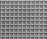
Pelcotec™ CDMS Critical Dimension Magnification Standards
The Pelcotec™ CDMS Critical Dimensions and Magnification Standards are made on an ultra flat silicon substrate with a precise 50nm chromium deposition for the features up to 5µm and a combination of 50nm gold over 20nm chromium for the features sizes from 2µm to 100nm. The Cr and Au/Cr on Si provides excellent contrast both in SE and BSE imaging mode. Read more...
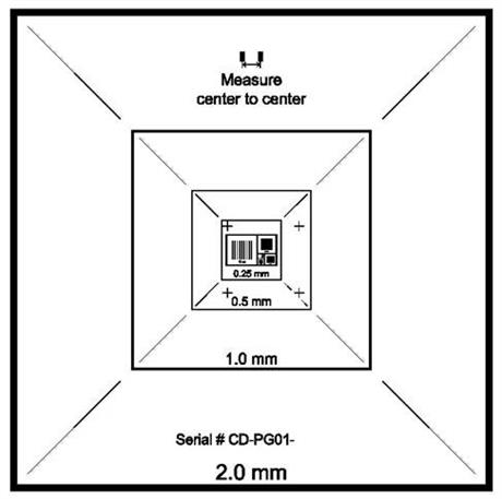
Art# 682-1 Pelcotec™ CDMS-1T; fully traceable with features from 2.0mm to 1um for a magnification range from 10x - 20,000x; ideal for desk top SEMs and low to medium magnification applications
They are available either unmounted or mounted on SEM holders A-R, see table here
Pelcotec™ CDMS-XY Critical Dimension Magnification Standards
The Pelcotec™ CDMS Critical Dimensions and Magnification Standards are made on an ultra flat silicon substrate with a precise 50nm chromium deposition for the features up to 5µm and a combination of 50nm gold over 20nm chromium for the features sizes from 2µm to 100nm. The Cr and Au/Cr on Si provides excellent contrast both in SE and BSE imaging mode. Read more...
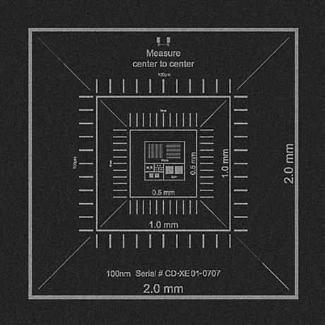
Art# 684-1 Pelcotec™ CDMS-XY-1T; fully traceable with features from 2.0mm to 1um for a magnification range from 10x - 20,000x; ideal for desk top SEMs and low to medium magnification applications
They are available either unmounted or mounted on SEM holders A-R, see table here
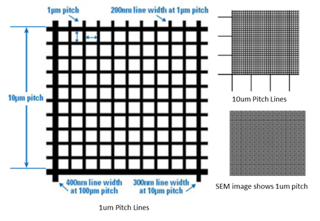
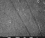
Pelcotec™ G-1 Silicon Calibration Specimen - 1µm Pitch Includes 1µm, 10µm and 100µm pitch
The Pelcotec™ G-1 calibration specimen with a 1µm pitch grid is very useful for magnification calibration or image distortion check in the 100x to 10,000x magnification range. Can be used for SEM, Auger, Sims, FIB, and LM (reflected light). Specimen may also be mounted directly on the Pelcotec™ G-1 which will give an accurate internal calibration in the image. Particularly useful when working with powders. Possible alternative for the SIRA calbration specimen (0.462µm pitch) which is no longer available.
The Pelcotec™ G-1 has the following specifications:
- Total calibration area is 3x3mm with a 1µm pitch grid
- Lines at 10um and 100um are thicker for easy orientation
- Includes 1µm, 10µm and 100µm pitch
- 300nm +/- 30nm deep line etched in ultraflat Si
- Line width is 200nm at 1µm, 300nm at 10µm and 400nm at 100µm pitch lines
- Precision is 1µm +/- 0.025µm with a perpendicularity better than 0.01°
- Serial number etched on each Pelcotec™ G-1 calibration standard
- NIST traceable version is Pelcotec™ G-1T
- Individually fully certified version is Pelcotec™ G-1C
- Si die size is 4x4mm with a thickness of 525µm +/-20µm, <100> orientation
- Boron doped silicon wafer with a resistivity of 5-10 Ohm/cm
- Available unmounted or mounted on SEM specimen mounts
Art# 633-1 NIST Traceable Pelcotec™ G-1T Calibration Standards.
Art# 633-11Individually Certified Pelcotec™ G-1C Calibration Standards.
Pelcotec™ LMS-20 Low Magnification Calibration Standard
The Pelcotec™ LMS-20 Calibration Standard has been specifically designed for precise low magnification calibration and specimen stage calibration. Useful for large area particle analysis, GSR analysis, low magnification SEM applications, and LM applications with reflected light. Useful in the 5x to 1000x magnification range.
Specifications are:
- Total calibration area is 20 x 10mm with crossed lines and 0.01mm divisions
- 75nm Cr lines on ultra-flat silicon substrate
- Cross hairs showed at every 0.1mm with larger cross hairs at 0.5 and 1mm over the complete area
- Serial number etched on each Pelcotec™ LMS-20 calibration standard
- NIST traceable version is Pelcotec™ LMS-20T (batch level certificate provided)
- Individually fully certified version is Pelcotec™ LMS-20C (individual certificate included)
- Si die size is 22 x 11mm with a thickness of 675µm +/- 10µm, <100> orientation
- Boron doped silicon wafer with a resistivity of 5-10 Ohm/cm
- Available unmounted or mounted on larger SEM specimen mounts
Art#688-1 Pelcotec™ LMS-20T, Low Magnification Calibration Standard, Traceable.
Art#688-11 Pelcotec™ LMS-20C, Low Magnification Calibration Standard, Certified
Planotec Silicon Calibration Specimen - 10µm Pitch
Useful for magnification calibration or image distortion check in SEM and LM.
Single crystal silicon, 5mm x 5mm. The squares repeat every 10µm (0.01mm). The dividing lines are about 1.9µm wide, formed by electron beam lithography. A broader marking line is written every 500µm (0.5mm) which is useful for light microscopy. Lines are etched, and approximately 300nm deep. Available unmounted or mounted on SEM specimen mounts. A certificate of calibration can be supplied for the Silicon Test Specimen at extra cost.
Many types of samples can be mounted directly onto the Silicon Test Specimen so that an internal calibration is obtained in the image.
Thickness: 675µm
Si crystal orientation: <100>
Wafer type: P-type/boron doped
Resistance: 1-30 Ohm/cm
Art# 615 Planotec Silicon Test Specimen
Art# 660-615-A Planotec Silicon Test Specimen certified
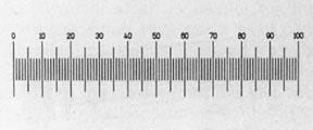
Low Magnification Calibration Ruler
100 markings, divisions 0.01mm on disc
Calibration ruler on 1/8" (3.2mm) nickel-plated copper disc. 1mm long scale with 100 markings, with 0.01mm divisions with an accuracy of +/- 0.0005mm or better. Available unmounted, or mounted on SEM mounts.
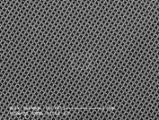
500nm SEM Cross Line Grating Replica
500nm cross line grating carbon replica (waffle pattern) with Au/Pd shadowing. Replica is mounted on a 400 mesh copper TEM grid with a diameter of 3mm. This cross line replica has well-defined trench type grooves, which makes it easy to determine the 500nm pitch or the 2,000 lines per millimeter. Available as unmounted standard or mounted on a SEM mount.
See our #253 Magnification Calibration slide-rule for quick assistance in obtaining magnification based on space counts of this product.
Grating Replica, Waffle
(Crossed-Lines)
Carbon replica with Au/Pd shadowing with 2,160 lines per millimeter. Replica is mounted on a 400 mesh copper TEM grid with a diameter of 3mm. See our number 252 Magnification Calibration Slide-Rule for quick assistance in obtaining magnification based on space counts of this product.
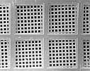
Fine Copper Mesh Grids in Folding Grids (unmounted)
For low magnification calibration of scanning electron microscopes. The fine mesh is held within a Ø3mm 100 mesh folding grid.
Available with 1000 mesh (25.4µm pitch).
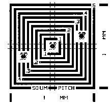
SEM Magnification Standard and Stage Micrometer MRS-4
The 10x to 200,000x standard for Scanning Electron Microscopy
with 1/2, 1, 2, 50 and 500µm pitch patterns and X & Y Micro-ruler
.
For ordering:
Art#614-821 MRS-4 Reference Standard, X, Not Traceable, without Protective Retainer, Unmounted
Art#614-822 MRS-4 Reference Standard, X-Y, Traceable, without Protective Retainer, Unmounted
Art#614-823 MRS-4 Reference Standard, X-Y-Z, Traceable, without Protective Retainer, Unmounted
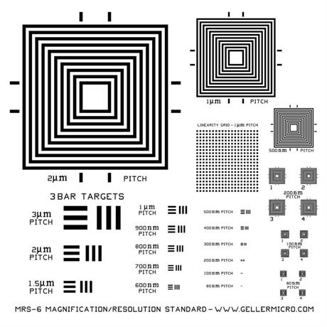
MRS-6 Magnification Reference Standard 1,500x - 1,000,000x
This is the next generation, NIST and NPL (NIST counterpart in the U.K.) Traceable, Magnification Reference Standard & Stage Micrometer. For Instrument Calibration from 1,500x – 1,000,000x (80nm min. pitch).
- Electron Microscopy: SEM and FIB/SEM (secondary & backscattered electrons), TEM (for use with a bulk holder) the MRS-6 is conveniently sized at 3.2 x 3.2 x 0.5mm.
- Scanning Microscopies and Profilometry: STM, AFM, stylus and optical, etc. The pattern height is approximately 15nm.
- Optical Microscopy: reflected, bright/dark field, differential contrast, and confocal.
- Chemical Mapping: EDS, WDS, Micro/Macro XRF, XPS, Auger, and others. The pattern is fabricated using 15nm chromium over single crystal silicon.
- Resolution Testing: With a series of 2 bar targets (similar to the USAF 1953 patterns) ranging in size from 80nm to 3µm.
- Linearity Testing: With a 1µm² pitch over 40 x 40µm.
- A Standard Ahead of Its Time: The MRS-6 represents a challenging next step. The nanotechnology sized patterns will be a good test of your imaging systems.
- Advanced optical microscopes now have submicrometer test patterns to measure resolution and linearity.
- Scanning electron microscopes have a pattern that will show significant differences between backscattered and secondary electron type I and type II images. Imaging the pattern will also tax their low accelerating voltage capabilities.
- Scanning probe microscopes have a pattern that is closely sized to the finest cantilever tips challenging their resolution ability.
Read more for detailed info here...
For ordering:
Art#614-80 MRS-6NT Reference Standard, X-Y, Not Traceable, without Protective Retainer, Unmounted
Art# 614-81 MRS-6XY Reference Standard, X-Y, Traceable, without Protective Retainer, Unmounted